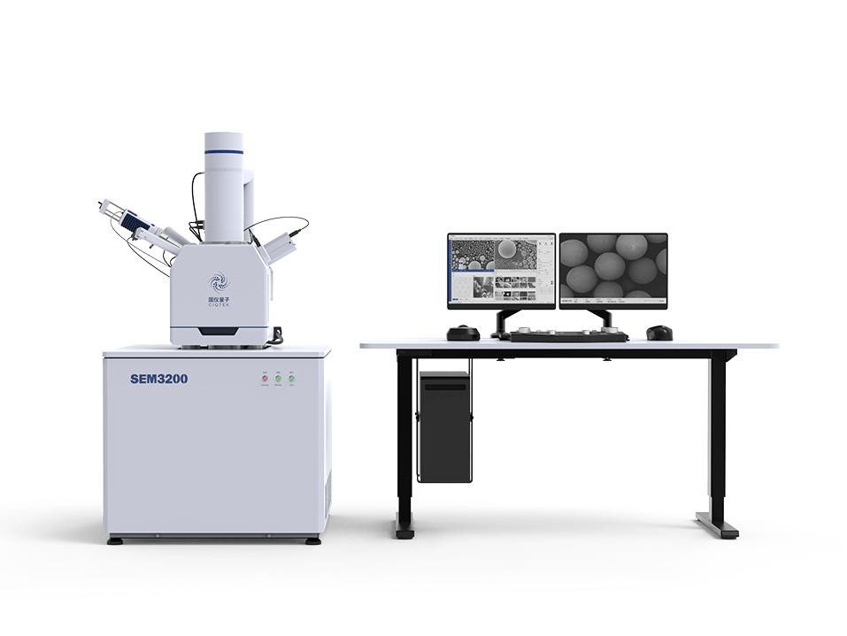
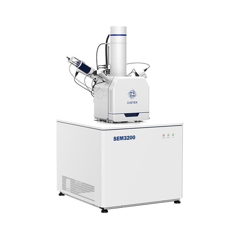
Tungsten Filament Scanning Electron Microscope | SEM3200
CIQTEK SEM3200 is a high-performance tungsten filament scanning electron microscope with excellent imaging quality
capabilities in both high and low vacuum modes.
It also has a large depth of field with a user-friendly interface to enable users to characterize specimens and explore
the world of microscopic imaging and analysis.
| Models | SEM3200A | SEM3200 | ||
| Electro-Optical Systems | Electron Gun | Pre-aligned Medium-sized Hairpin-type Tungsten Filament | ||
| Resolution | High Vaccum | 3 nm @ 30 kV (SE) | ||
| 4 nm @ 30 kV (BSE) | ||||
| 8 nm @ 3 kV (SE) | ||||
| *Low Vaccum | 3 nm @ 30 kV (SE) | |||
| Magnification | 1-300,000x (Film) | |||
| 1-1000,000x | ||||
| Acceleration Voltage | 0.2 kV ~ 30 kV | |||
| Probe Current | ≥1.2μA, Real-time display | |||
| Imaging Systems | Detector | Everhart-Thornley Detector (ETD) | ||
| *Backscattered electron detector (BSED), *Low vacuum secondary electron detector, *Energy spectrometer EDS, etc. | ||||
| Image Format | TIFF, JPG, BMP, PNG | |||
| Vacuum System | Vacuum Model | High Vacuum | Better than 5×10⁻⁴ Pa | |
| Low Vacuum | 5 ~ 1000 Pa | |||
| Control Mode | Fully Automated Control | |||
| Specimen Chamber | Camera | Optical Navigation | ||
| Monitoring in the Specimen Chamber | ||||
| Specimen Table | Three Axis Automatic | Five Axis Automatic | ||
| Stage Range | X: 120 mm | X: 120 mm | ||
| Y: 115 mm | Y: 115 mm | |||
| Z: 50 mm | Z: 50 mm | |||
| / | R: 360° | |||
| / | T: -10° ~ +90° | |||
| Software | Operating System | Windows | ||
| Navigations | Optical Navigation, Gesture Quick Navigation | |||
| Automatic Functions | Auto Brightness & Contrast, Auto Focus, Automatic Stigmator | |||
| Special Functions | Intelligence Assisted Image Astigmatism Correction *Large-FOV Image Stitching (Optional) | |||
| Installation Requirements | Temperature | 20°C (68°F) ~ 25°C (77°F) | ||
| Humidity | ≤ 50 % | |||
| Power Supply | AC 220 V(±10 %), 50 Hz, 2 kVA AC 110V(±10%), 60Hz | |||
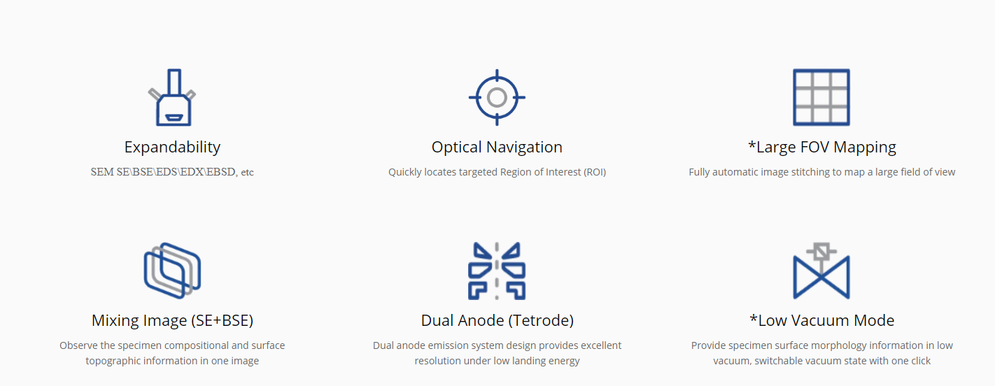
Versatile Detectors
The scanning electron microscope (SEM) is used not only for the observation of surface morphology but also for the analysis of the composition of micro-regions on the specimen surface.
CIQTEK SEM3200 has a large specimen chamber with an extensive interface. In addition to supporting conventional Everhart–Thornley detector (ETD), Backscattered-Electron detector (BSE), and Energy-dispersive X-ray spectroscopy (EDS/EDX), various interfaces such as Electron Backscatter Diffraction Pattern (EBSD) and Cathodoluminescence (CL) are also reserved.
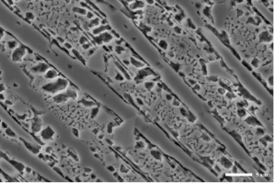
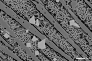
Backscattered-Electron Detector (BSE)
Comparison of secondary electron imaging and backscattered electron imaging
In the backscattered electron imaging mode, the charge effect is significantly suppressed and more information on the composition of the specimen surface can be observed.
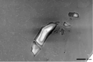
Plating Specimens:
Tungsten Steel Alloy Specimens:
Four-quadrants Backscattered Electron Detector - Multi-channel Imaging
The detector has a compact design and high sensitivity. With the 4-quadrants design, it is possible to obtain topographic images in different directions as well as composition distribution images without tilting the specimen.
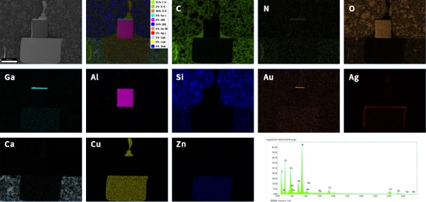
Energy Spectrum
LED small bead energy spectrum analysis results.
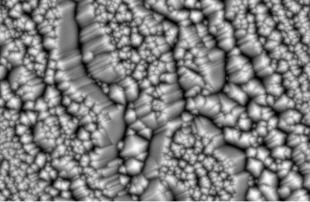
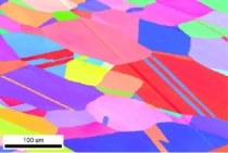
Electron Backscatter Diffraction Pattern (EBSD)
The tungsten filament electron microscope with a large beam current fully meets the testing requirements of high-resolution EBSD and can analyze polycrystalline materials such as metals, ceramics, and minerals for crystal orientation and grain size analysis.
The figure shows the EBSD grain map of Ni metal specimen, which can identify grain size and orientation, determine grain boundaries and twins, and make accurate assessments of material organization and structure.
 SEM
SEM
| Prod# |
|---|
| SEM3200 |
| Description |
|---|
| CIQTEK Tungsten Filament Scanning Electron Microscope |
| Unit |
|---|
| each |
| Price |
|---|
| P.O.R |
| Order/Quote |
|---|
| Qty: Add to cart |
| Prod# | Description | Unit | Price | Order/Quote |
|---|---|---|---|---|
| SEM3200 | CIQTEK Tungsten Filament Scanning Electron Microscope | each | P.O.R | Qty: Add to cart |